
VGA 2.0: First fire-up of the basic circuit -- it's not pretty :)
- rehsd

- Mar 6, 2022
- 3 min read
Updated: Mar 7, 2022
I have fired up the basic circuit for my VGA 2.0 (320x240x1byte). I can't say it's pretty, but it's at least outputting something. Now, on to the troubleshooting and rework phase...
The first things that I notice:
The full image isn't being displayed. It appears that the image is partially displayed, and at a certain vertical point (roughly mid-way down on the screen) the image starts over. I'm guessing this is either how I'm decoding from the ROM or a counter/timing issue. This is my primary concern at this point. I need to figure out why I'm seeing this behavior. I can shift the vertical counters used on the ROM and get the full image displayed, but it's at normal vertical resolution, so it takes up half the screen vertically. I'm hoping to have 320x240 stretched vertically to take the entire screen (which is running at 640x480).
There are vertical white lines. I've seen others mention in the past that this might be caused by the access speed on the ROM. I'm not sure yet if that's this specific cause here. Interestingly, one of the white lines is missing.


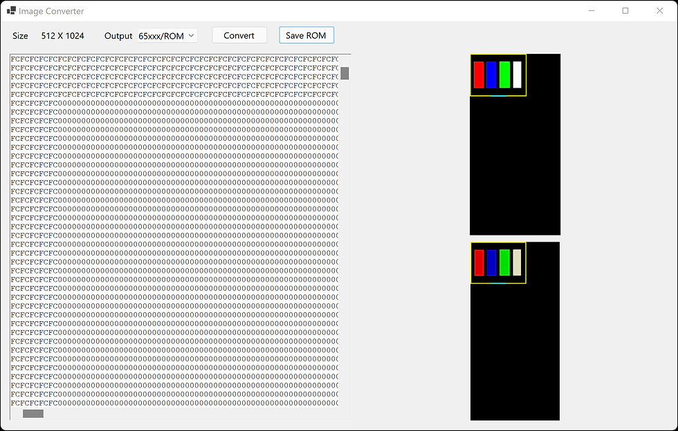
Here's a cropped version of the image I have saved on the flash ROM. The full image is 512x1024 with color compressed down to a single byte per pixel. In this image below, I have cropped the bottom of the image that is just black.


Note: In the schematic above, the red signal after the resistors should go to pin 1 of the DSUB and the blue signal should go to pin 3. Green should remain in pin 2.
Associated logic for the two PLDs:


Scope of VSync and HSync signals:


To quickly compress the color space for test images, I wrote a small Windows forms application that lets me pick an image and compressed the color data from 4 bytes (ARGB) down to a single byte (RRRGGGBB), saving it in a binary file to quickly load into the ROM programmer. It provides a preview of the before and after, also.

Updates

-I updated my horizontal PLD logic slightly. I referenced my VGA 1.0 design for the SR latches. I remember having issues with Ben's schematic, specific to the latches.
-I notice that Q9 on my vertical counter is showing up as 60Hz on my scope (the same as Q8). I would expect Q9 to measure at 30Hz, but maybe that's not right. Maybe the vertical counter reset is happening too quickly, and I shouldn't read anything into it.


-As I'm digging into the issue of the image only being displayed halfway vertically, I am looking at my ROM addressing. This addressing is coming from a combination of vertical and horizontal counters. To help me illustrate it, I put together the following graphic. In the process, it seemed to be clear that I need one more bit on my vertical addressing (i.e., add vertical Q8 to ROM A16 (instead of tying it to ground as it is now). Anyways, below is the mental exercise that helped me come to that conclusion. I will add this additional counter to the logic and see if it resolves my vertical issue.

And with the addition of Q8:

Updated ROM addressing schematic:

Updated schematic and PLD logic:


Based on a suggestion from u/gfoot360 (thank you!), I added a 74HC273 to the output of the ROM. This helped reduce the vertical lines.


PDF version of the schematic at this point:
Next
I have plenty of wiring cleanup to remove the temporary jumpers. Then, I'm going to see if I can get my dual-port SRAM working to replace the flash ROM (and of course, get it connected to my 65816).


Comments