
16-bit Processor Build - Design Work, part 1
- rehsd

- Jul 20, 2022
- 9 min read
Updated: Aug 15, 2022
As I have my VHDL-based prototype of my 16-bit processor running, I am now starting the design work on an actual hardware implementation. Below are the initial PCBs I have been designing. A lot more work is needed, but I thought I would share where I am currently at. As always, feedback and suggestions are welcome! I guarantee countless aspects of this build can be improved.
I will update this page as the designs are solidified.
Bus
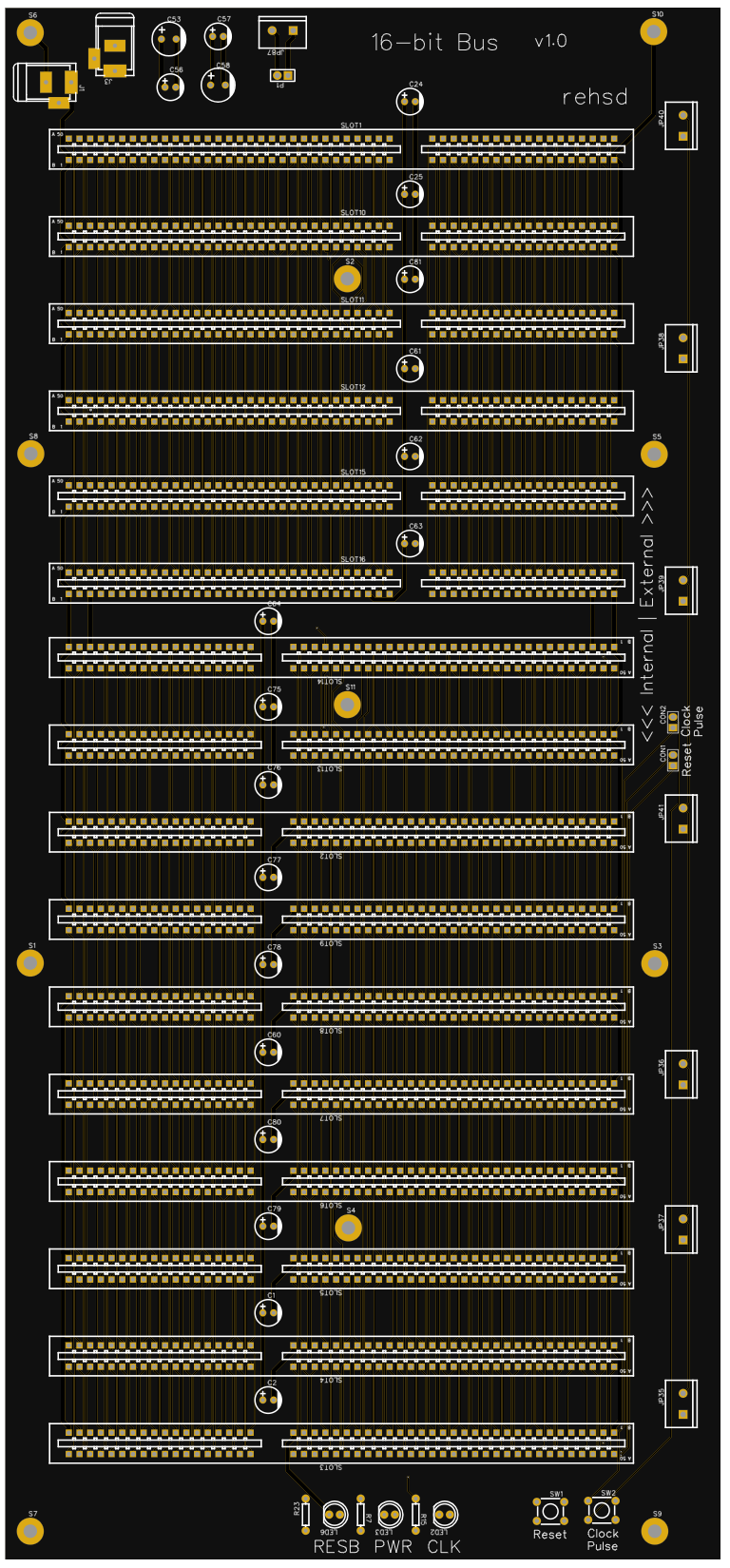
The bus board contains two independent buses. The first bus is for the 16-bit processor itself (internal). The second bus allows connectivity with add-in cards from my 65816 system (external). The physical connections are ISA slot connections (no ISA protocol). I have a bunch of ISA slot connectors from my 65816 system build, and I have found the connections to be quite handy. I will bridge these two buses through the ROM/RAM card, exposing the necessary signals to the external bus (e.g., address, data, read/write, reset, and clock). It is surprising how quickly I used up available connections on each of the buses. 😕 This will be a two-layer PCB. I have increased VCC and GND traces from 0.254mm to 1mm. I do not plan to include bus terminating resistors in the initial version. This could potentially limit speeds, but I am more worried about basic functionality at this point. Cost per PCB: ~$6 (USD).


I am breaking up the functionality of the 16-bit processor into a series of add-in cards. I am maintaining the same width for all cards. I will extend the height of cards if necessary. So far, I have had to increase the height of one card. I am hoping to keep everything within the bus board width and length (170mm wide by 353mm long -- or 6.7" by 13.9").
Clock, System Reset
The clock can either run from a 555-based timer, single step, or from a full can oscillator. This will be a two-layer PCB. Cost per PCB: ~$2.

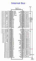
Microcode, Flags
The design supports 48 control bits. As of this writing, I am using 36 of those bits. I only have two flags so far: zero and carry. A small ribbon cable will connect between this card and the following card (Counters, Instruction Register, Reset State), bringing over instruction and step signals, which are used with the two above flags to retrieve the appropriate control signals from the flash. This will be a four-layer PCB, with all four layers for signal. The PLCC flash chips increase the challenge of signal routing. Cost per PCB: ~$9.

Counters, Instruction Register, Reset State
This card includes the program counter, step counter, instruction register, and SR latch for the startup reset flag. This card has a small interconnect with the microcode card above (see note there). This will be a four-layer PCB with two inner signal layers. Cost per PCB: ~$8.50.

Registers
Initially, I was looking at some SSOP and TSSOP ICs for flip-flops and bus transceivers. I found the routing to be a bit painful, so I am going with different DIP ICs instead (at least for now). At some point, I may try a surface-mount edition of this card. This will be a four-layer PCB with a GND plane and an inner signal layer. The system will use at least two of these cards, if not three. Cost per PCB: ~$8.50.

Shift, Rotate, AND, OR
This card supports 16-bit shifting and rotating -- left and right -- along with AND and OR bitwise operations. The 'I' register is also included on this card. This will be a two-layer PCB. Cost per PCB: ~$2.50.

ROM, RAM, Decode Logic
This card has the core ROM, RAM, and address decode logic. It includes an initialization ROM (32 Kx16 usable), primary ROM (32 Kx16 usable), static RAM (28 Kx16 usable), and decode logic. ROM ICs are x16 (i.e., two bytes per address). A pair of x8 SRAMs will be used to offer x16 per address. This board will have a corresponding daughter card that will interface with the external bus -- basically a bridge from the 16-bit processor to the external slots for video, sound, or other I/O. The daughter card will either connect through pin headers or a ribbon connection. This will be a four-layer PCB with two inner signal layers. Cost per PCB: $8.50.

Bus Bridge Card
This card connects the internal bus to the external bus, leveraging a 50-pin ribbon between this card and the ROM/ROM card (above). I am not yet sure how the ribbon cable may impact maximum clock speeds. On my 65816, I use a dev board that is connected through a ribbon cable; it seems to perform just fine, without being the bottleneck for maximum clock speeds. This will be a four-layer PCB with two inner signal layers (due to significant crossover of signals from the ISA connector to interim jump blocks to the ribbon connector). Cost per PCB: $8.50.

Bar Graph Debug Module

For cards that include signals I would like to visually see, I will include headers to connect a small debug module. This module contains bar graphs and associated resistors to display the signals. These can be easily added and removed from the cards. Since they connect to a right-angle pin header on the card, they are visible even when all cards are inserted into the bus board. This will be a two-layer PCB. Cost per PCB: $0.30.
Add-in Cards from 65816 System
I mentioned earlier that I am looking to support the add-in cards from my 65816 system in this 16-bit processor system. One challenge will be addressing. My 65816 system has a 16 MB address space, while this 16-bit system only has 64 KB. My video card, for example, uses 128 KB of RAM, so this may be difficult with a 64 KB address space.
My plan for the video card is to drop the resolution down from 320x240 to 256x240 and add an instruction (and control line) to the 16-bit processor to write to the video card. For example, I will use STV (store to video) as an instruction, and this instruction will use a control line that enables the video RAM for writing. With the resolution of 256x240, I can drop one of the memory daughter cards on the video card and run 64 KB of video memory. This will allow me to access to full video memory of 64 KB.
For my sound card, I may do something similar -- add a control line and instruction of STS (store to sound) -- that allows me to control the sound card.
I will need to develop a new I/O card for the external bus that includes PS/2 keyboard input. Possibly, I could add USB mouse and NES controller input to the same card.
Additional Thoughts
All of the PCBs above require additional validation, general clean-up, and silkscreen work. I have not added filtering caps for all ICs on all boards. For boards that are four-layer boards, I may put more effort in getting them down to two-layer boards. I am also going to try an increase the width of all VCC and GND traces.
It is looking like total PCB cost for the 16-bit system is going to come in around $65 per system (having to order five of each, and with shipping/handling... out-of-pocket approaching $400... ouch... 😢). This does not include any of the add-in cards from my 65816 system or components to populate the 16-bit processor PCBs. I suppose I could have other hobbies that are more costly. 😂
Address Decode Logic
I will use a GAL22V10D to manage address decode logic. My current plan:

Current Instructions, Registers, and Control Lines
Here's a snapshot of the processor's current support:

Schematics
Version 0.01. 🙃
ICs Used
My counting might be slightly off, but this should be close:
555 - qty 4
74HC00 - qty 13
74HC02 - qty 1
74HC04 - qty 1
74HC08 - qty 2
74HC14 - qty 5
74HC20 - qty 1
74HC32 - qty 13
74HC74 - qty 1
74HC139 - qty 3
74HC161 - qty 6
74HC173 - qty 32
74HC245 - qty 60
74LS279 - qty 1
AT49F1025-70 - qty 5
GAL22V10D - qty 1
IS61C256AH - qty 2
Update: PCB Initial Order (small subset of PCBs)
I have completed clean-up of the PCBs and added to them to my shopping cart. $$$
As I have not yet vetted all of the circuits, and the total cost of the PCBs is adding up to be quite high, I am going to pause here. I ended up making many of the PCBs four-layer, either to support power distribution (bus board) or to help with more complex signal distribution. Before committing my fun money for the foreseeable future, I want to do my best to remove errors before ordering. 🙂

I have ordered the necessary ICs to validate my design, and those parts will take a few weeks to arrive. Additionally, I have ordered the dual bus PCB, the clock/reset PCB, and some bus-to-breadboard adapter PCBs. I plan to test my design for the other PCBs and order those later, likely late August.


The black PCBs directly above have been manufactured, loaded, and tested. See 16-bit Processor Build.
Update: PCB Order #2
I have ordered the next PCB in my list -- the PCB for the program and step counters, instruction register, and reset status. I made several adjustments to the schematic prior to ordering (compared to the originally-posted draft schematic listed above); see updated schematic below. I want to use this board to test my approach to registers and bus access. This will also let me test the LED debug headers.


I have also ordered a modified version of the Control/Flags PCB. The x16 flash ICs I was hoping to use are not supported by my TL866II Plus programmer. I am going to start out with a version that uses AT28HC256-70 EEPROMs. Later, I may build a smaller version of the PCB with the AT49F1025-55JC flash memory.

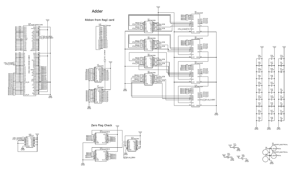
Missing Adder!
Somewhere along the way, I forgot to build a circuit for the adder. I plan to create an additional card that handles addition, subtraction, and setting the carry and zero flags.
IC for System ROM
For the control card, I moved away from the x16 flash memory due to programming challenges (at least near-term). The traditional DIP EEPROMs will work just fine for control signals for now. However, for my system ROM, I really do want to use x16 flash storage. I will have some work to do for this to be supported. I may need to build a custom PCB that allows me to use my PLCC44 flash memory in my TL866II Plus programmer. (The standard PLCC44 to DIP40 adapter for my programmer does not have the appropriate pinout for this programming.) I may then use a ZIF socket on the ROM card, inserting the same adapter PCB into the ZIF. A downside to this approach is the space required, as it will use up two slots on the bus board due to the total width of the card. I am going to keep thinking about options here. I could use a pair of x8 flash ICs, too, updating my assembler to create a pair of ROM images (split for MSB and LSB for each address).

Update: I ordered this PCB to allow me to program the x16 flash memory ICs. It should allow my programmer to treat the ATF1025 PLCC44 as an AT49F1024 VSOP40. I will try this out with my programmer, and if it works, use it in a breadboard version of the RAM/ROM card. If that all goes fine, I plan to update the RAM/ROM card with a ZIF socket and use this adapter. This will allow me to much more easily reprogram the flash memory.
I also updated the ROM/RAM card to support the primary ROM in either the PLCC or the adapter pictured above in a ZIF socket. The initialization ROM will likely never need its contents updated, so the PLCC44 socket is fine. Having the dual option for the primary ROM might also provide some flexibility of performing in-board reprogramming of the primary ROM, through the ZIF socket pins (something for me to test later).

Update - Adder PCB Initial Design
This card will support adding/subtracting, provide the carry flag, and check for zero on the A register, setting the zero flag accordingly. The flag is stored on the microcode card when the "flags in" control is set. This is a two-layer PCB.

Update: PCB Order #3
I have ordered the following PCBs:
Bus Extension card (version 1.2) and associated breadboard adapters. This version provides better granularity for splitting bus signals out to breadboards.
Bus Debug card for writing to and reading from the 16-bit bus. This will be my first PCB with a surface mount IC -- and it is a TSSOP, so this will definitely challenge my soldering skills.
Bus Termination card. This will allow me to experiment with different bus termination, including Thevenin, with simultaneous pull up and pull down (this worked well on my 65816 motherboard). The card also exposes headers for bus signals, similar to the bus extension card.


Update: PCB Order #4
I have ordered the following PCBs:
Dual 16-bit Register card. This card contains two 16-bit registers and supports jumper wires to select which registers are handled on each card (e.g., A, X, Y, I, J, PC). I cut the card down to two registers instead of three registers so that I could get away with a two-layer PCB.
RAM, ROM, Decode card. This card contains 32K x 16 RAM, 32K x 16 ROM for initialization, 32K x 16 ROM for post-initialization, and a GAL22V10D for address decode logic. At some point, I hope to use AT49F1025-55 flash instead of the EEPROMs. However, I am waiting on an adapter to be able to program the flash, and it will likely be a month out. This card also sends necessary signals to the Bus Bridge card to transfer to the external bus. With the change to the DIP EEPROMs, I was able to drop down from four-layer to two-layer PCBs.
Bus Bridge card. This card takes signals from the RAM, ROM, Decode card and places the signals on the external bus. The external address and data values are also viewable from the LED debug modules on the card. I removed the cross-bus pin headers and was able to reduce the card to a two-layer PCB.


As this page has gotten a bit long...


Comments