
16-bit Processor Build - Design Work, part 2
- rehsd

- Aug 15, 2022
- 3 min read
Updated: Sep 28, 2022
Continued from 16-bit Processor Build - Design Work, part 1...
Currently-planned Instructions
My current plan is to have approximately 40 instructions supported by the processor in the initial build. This number will grow in time, I think. Below is a link to a PDF with a list of instructions, their hex values, steps, and the control signals per step. Instructions can range from one to eight steps. Control signal 25 (C25 STPR) is flagged for the last step of an instruction and causes the processor to move to the next instruction in code. This provides support for variable-length step count. I notice that I do not have this flag set for all instructions yet, but I will make updates as I work to optimize the instructions. Any row with all control flags set to 0 means that step is not required. Some steps are tweaked to work in my FPGA-version of the processor (e.g., duplicate calls due to FPGA timing). There is room for improvement yet.
Examples: LDXI (load X immediate) requires 5 steps, LDXA (load X absolute) requires 5 steps, JMPA (jump absolute) requires 4 steps, ROL (rotate left) requires 3 steps. Each step translates to a clock cycle.

Full instruction list (as of 15 August 2022):
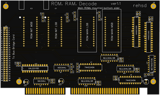
PCBs Incoming: Shift/Rotate/And/Or, Add/Subtract, & Updated ROM/RAM/Decode
I have the core system running now. See 16-bit Processor Build - Initial Assembly. I made some updates to the ROM/RAM/Decode card. I have ordered the updated PCB along with two new PCBs. I have one PCB that processes shifting and rotating, left or right, and also handles bitwise AND and bitwise OR. Additionally, I have a PCB coming to handle adding, subtracting, setting the carry flag, and setting the zero flag.


If I can get these additional cards running properly, I should have enough functionality to drive a 1602 LCD as a real-world test of the 16-bit processor.
Updated Control Card
I updated the design of the microcode/control card. I removed the LED debug headers to simplify routing and get the board down to a two-layer board. I also replaced the AT28C256 EEPROMs with SST39SF040A flash. The primary reason I swapped out the EEPROMs is to add additional address bits, so that I have room for more control flags to control the output. An additional benefit to the flash is that they are more readily available and at a lower cost. Finally, I added a 74HC245 bus transceiver to the output of each flash to improve its bus transmission. With current testing, I have found that the '245 works quite well on an overly-extended (in length) bus, while the EEPROMs struggle. I expect the flash behavior is more in line with the EEPROMs and looking to the improve the bus transmission.
I designed a new PCB to show bus and control signals. This is a simple two-layer PCB that can be used while debugging.


Improved Stack Pointer Support
I designed this card to act as a register for the stack pointer and to all be able to provide the addresses of previous and next entries in the stack. This will be required for JSR and RTS instructions.


Updated Bus Bridge
I have updated the bus bridge card to spread out the debug headers for LED bar graphs. I also added additional connections for connecting the Arduino logger. I included a couple of spots for ICs in case I need to add something.

Interrupt Support
This is a first attempt at adding support for interrupts. The interrupt vector can be set to any address between 0xFF00 and 0xFFFE. I included a couple of spots for ICs in case I need to add something.

Updated Bus Board
To support additional internal bus slots, I have removed the external bus from the board. I have also dropped down to two-layer instead of four-layer. I will connect a separate external bus PCB via an interconnect of some sort (ribbon for now).

Current "Internal" and "External" Buses
Here are the current signal pinouts of the internal ISA slots and external ISA slots. As a reminder, I am not following the ISA protocol specification; rather, I am simply using ISA physical connectors. The left image is of the internal bus for the processor. The right image is the external bus, now separate from the main bus board. On the internal slot, I wish I could also fit Register I, as I use Register I for several different instructions. Possibly, I will expand the design with an additional connector for each card to support Register I (currently, I am using ribbon cables to share Register I amongst some of the cards).


More to come...


Comments