
W65C265S Parallel Interface Bus (PIB)
- rehsd

- Jan 7
- 5 min read
Updated: 4 hours ago
As I've been working on my W65C265S single-board-computer (SBC) project (see rehsdonline.com/post/w65c265s-single-board-computer), one of the greater mysteries is the parallel interface bus (PIB). I've found limited information about the PIB, other than some basics in the '265 data sheet. I'm hopeful to get the PIB implemented in the latest phase of my '265 SBC project. Here, I will collect information that should be helpful in my goal of implementing PIB for a dual-265 SBC. As of this writing, I have an updated PCB designed that might support PIB.
The general design intent is to have a primary '265 microcontroller with a secondary "co-processor" for audio-visual tasks (I'll refer to the secondary MCU as my AV-265). These tasks include managing the VGA output and audio output (using a pair of YM2149 programmable sound generators). The primary controller can submit simple requests to the AV-265 and continue on with other work, while the AV-265 grinds through screen draws and playing audio.

As I start this blog post, my latest schematic is microcontollers/W65C265S/65265 schematic 20260107.pdf at main · rehsd/microcontollers · GitHub.
This post will be updated as I work through the PIB design of my SBC.
Some of the information here is speculation, or me "reading between the lines" due to limited documentation. If you see anything that is incorrect, please let me know so that I can correct it.
PIB Information from Western Design Center (WDC)
Here, I am capturing information that WDC has published on the PIB. In the subsequent section, I will capture my interpretation and implementation.
3.21 Parallel Interface Bus (PIB)

2.10 Parallel Interface Bus (PIB)

Parallel Interface Registers

Parallel Interface Bus Enable Register (PIBER)

Parallel Interface Bus Flag Register (PIBFR)

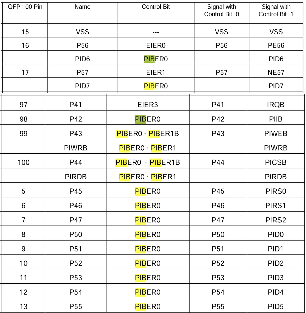
W65C265S 100 Lead QFP Chip Carrier Pinout

Communication Register Map

Memory Map


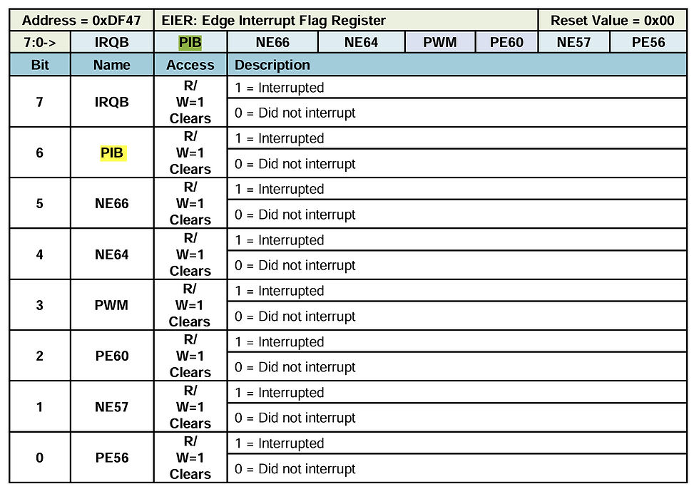
Edge Interrupt Enable Register (EIER)

Edge Interrupt Flag Register (EIFR)
Native Mode Priority Encoded Interrupt Vector
Address: 0xFF9C,D
Label: IRQPIB
Function: Parallel Interface Bus (PIB) Interrupt
Information from Other Sources
Placeholder... not much out there!
If you know of additional information sources, please drop me a note! Thanks!
My Implementation
Here, I will share my interpretation and implementation.
The term master is synonymous with host, and the term slave is synonymous with processor.
Here is what I am thinking for connectivity of the two '265 MCUs.

Below, I list considerations related to the connections in the image above.
Pin | PIB Use | Other Functions |
P42 | PIIB (Parallel Interface Interrupt) The PIB interrupt output to the "host" is generated on the Parallel Interface Interrupt (PII) pin. The "host" interrupt is suggested to be received on the IRQ level interrupt input pin of the "host" processor. | None |
P43 | PIWEB (Parallel Interface Write Enable) / PIWRB (Parallel Interface Write Register?) The Parallel Interface Write Enable (PIWEB) input pin is used with the Parallel Interface Chip Select (low active)/Parallel Interface Chip Select (high active) (PICSB/PICS) signal to transfer data to and from the Parallel Interface Register selected by the Parallel Interface Register select (PIRSx) input pins. When PIWEB and PICSB are configured by the Parallel Interface Bus Enable Register bit 1 (PIBER1=0), then the PIB interface is compatible with WDC microprocessor WE- logical operation with the chip select PICSB input. The use of PIWEB and PICS are configured by PIBER1=1. | FA15 Used on SXB for external ROM bank select. This is an issue. |
P44 | PICSB (Parallel Interface Chip Select low active) / PICS (Parallel Interface Chip Select high active) PIRDB (Parallel Interface Read Data?) See notes on P43. | AMS Used on SXB for external ROM bank select. This is an issue. |
P45 | PIRS0 (Parallel Interface Register Select) | None |
P46 | PIRS1 (Parallel Interface Register Select) | None |
P47 | PIRS2 (Parallel Interface Register Select) | None |
P50 | PID0 (Parallel Interface Data bit 0) | DTRB0 |
P51 | PID1 (Parallel Interface Data bit 1) | DSRB0 |
P52 | PID2 (Parallel Interface Data bit 2) | DTRB1 |
P53 | PID3 (Parallel Interface Data bit 3) | DSRB1 |
P54 | PID4 (Parallel Interface Data bit 4) | DTRB2 |
P55 | PID5 (Parallel Interface Data bit 5) | DSRB2 |
P56 | PID6 (Parallel Interface Data bit 6) | DTRB3 If connected to the FT232 and using UART3 with RTS/CTS, this may be an issue. |
P57 | PID7 (Parallel Interface Data bit 7) | DSRB3 If connected to the FT232 and using UART3 with RTS/CTS, this may be an issue. |
P60 | GPIO on Master to pull down RESB on slave to keep slave under reset until Master has PIB enabled. |
While I have a PCB designed and ready to be ordered using the above connectivity, I am somewhat guessing at this connectivity. Given that, I am looking to test this using my first revision of a '265 SBC and a WDC W65C265SXB. I have recently moved all peripherals off of ports 4 and 5 to free up these ports for PIB. I'm starting with this...

Above, the green board is my custom PCB (round one), and the red PCB is WDC's W65C265SXB. On the right side, I have a versatile interface adapter (VIA) to support PS/2 keyboard data input and 1602 LCD output.
Schematic & Source Code: microcontollers/W65C265S/Pseudo-PIB at main · rehsd/microcontollers · GitHub
David L. offered a suggestion in the video comments for the above video. He suggested trying out Google Gemini (AI) to see what additional information it would return. Gemini provided the following extremely helpful details:
The W65C265S architecture is hard-wired for a "Host-to-Peripheral" relationship. In WDC's design, the PIB logic is a passive listener; it is built to respond to signals, not to generate them.
The W65C265S was intended to be a "smart" companion chip. WDC envisioned a system where a large CPU (the Master) would talk to the '265 (the Slave) to offload tasks like handling serial ports or pulse-width modulation. The Master is assumed to be a powerful CPU that can easily spare the few instructions needed to toggle a port. The Slave (the '265) is given "Auto-Handshake" hardware so it can catch high-speed data from the Master without dropping bytes, even if it's busy doing other tasks.
In other words, the '265 does not have hardware for PIB master functionality -- just slave functionality. I updated my project to leave PIB disabled on the master, with manual control signal management. This includes adding the mailbox number (PIR#) to the control lines on port 4 (top three bits). I updated the slave code to enable PIB with automatic handshaking and the PIB interrupt. Success!
Schematic & Source Code: microcontollers/W65C265S/PIB working at main · rehsd/microcontollers · GitHub
Ultimately, this connectivity works for my setup:

[February 26, 2026] I now have PIB running on my Primary+AV build!
Code for the above video: microcontollers/W65C265S/Primary AV Boards/65265 assembly FULL 20260226 - PIB at main · rehsd/microcontollers · GitHub
More to come!
Comments